


by Arpan Sow
The Strategic Reality AI foundational models aren't neutral - they embed the values, languages, and priorities of their creators. The US, China, and EU understand this: whoever controls foundational models controls global discourse and decision-making.
India, despite 1.4 billion people and world-class tech talent, remains on the periphery because it lacks the fundamental infrastructure to build sovereign AI.
The Compute Bottleneck: Numbers That Matter Training a 600-billion parameter multimodal model requires:
20,000-30,000 NVIDIA H100 GPUs running for 60 days
36 sextillion FLOPS of computation
Example: xAI's Grok 3 used 100,000 H100 GPUs, consuming 200 million GPU-hours
As AI evolves toward physical robotics and autonomous systems, these demands will only intensify. OpenAI's "Stargate" initiative plans continental-scale supercomputers for artificial general intelligence.
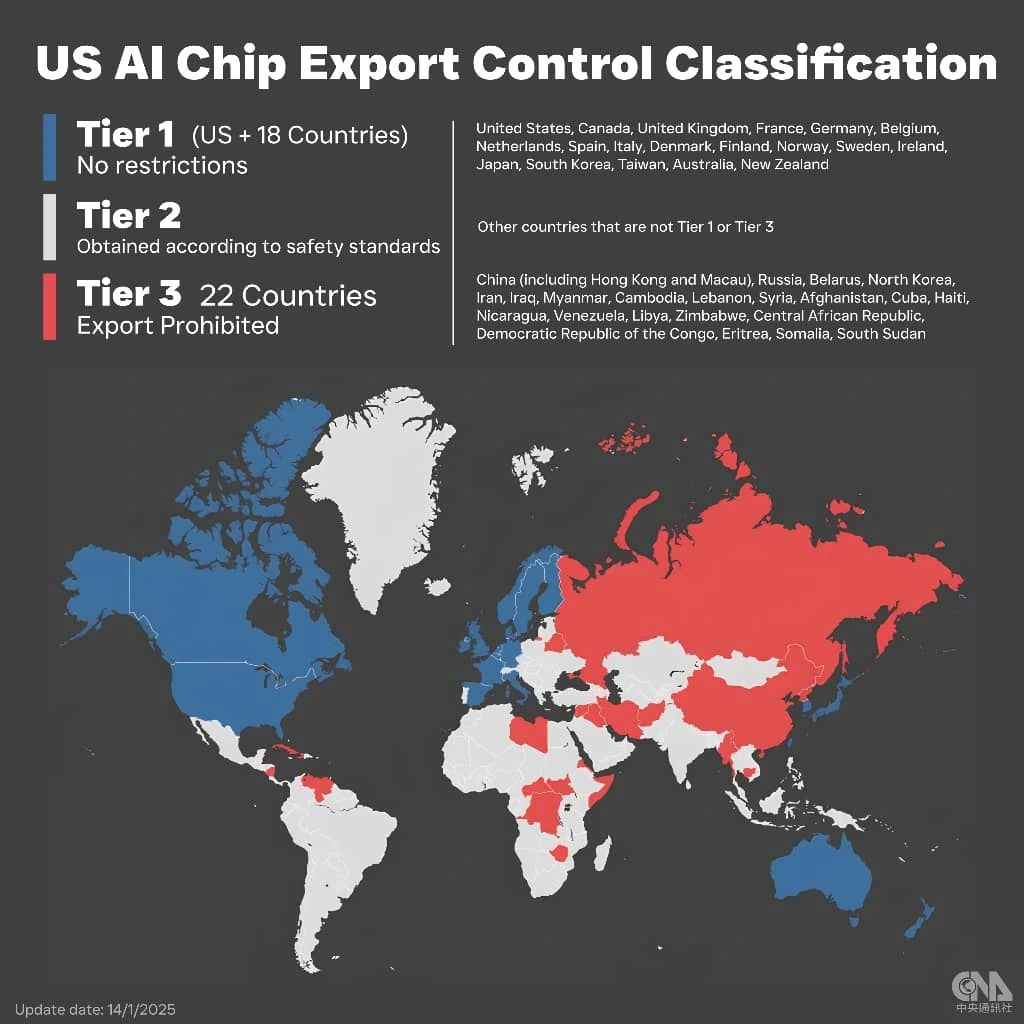
The Semiconductor Stranglehold The US operates a three-tier export system:
Tier 1 (UK, France, EU): Minimal restrictions on high-end AI chips
Tier 2 (India): Highly regulated, ~100,000 AI chip annual cap
Tier 3 (Russia, China): Severe restrictions or outright denial
India faces potential relegation to Tier 3 as geopolitical dynamics shift. NVIDIA's dominance compounds this vulnerability - they maintain massive backlogs with US companies getting priority, leaving countries like India as secondary customers.
China's $130 Billion Lesson China anticipated US restrictions and built comprehensive domestic capabilities:
Industrial Infrastructure:
Manufacturing equipment: SMEE, AMEC, Naura Technologies
Design tools: Empyrean, Xpeedic, Primarius (competing with Siemens/Cadence)
Chip companies: Huawei (Ascend series), Moore Threads, Lisuan
Strategic Approach:
"Big Fund" 3.0 targets entire supply chain: design, manufacturing, packaging, testing, equipment, materials
Rapid feedback loops between toolmakers and strategic companies (SMIC, Huawei, YMTC)
Innovative approaches: developing EUV mirrors through space-based solar X-ray imaging projects
Result: Chinese companies now just one generation behind NVIDIA.
India's Technical Pathway
Design Foundation:
GPU architecture fundamentals for AI/HPC workloads
OpenLane platform: integrates Yosys (RTL synthesis), OpenROAD (placement/routing), Magic/Netgen (verification)
Computational photolithography tools: LithographySimulator, Optolithium, OpenILT for predicting/optimizing chip patterns
Fabrication Capabilities:
EUV Light Sources: BARC's Accelerator Division (Dr. Amitabha Roy) has soft X-ray expertise; EUV falls in 10-100nm soft X-ray band
Laser Systems: DRDO fiber laser technology for heating tin droplets
Precision Mirrors: BARC's Atomic & Molecular Physics Division has multilayer mirror experience for X-ray applications
Positioning Stages: Magnetic levitation technology for nanometer-level wafer placement (research by Dr. P. Ananthababu, Dr. K.S. Vikrant)
Inspection Systems:
Electron microscopy for defect detection (open-source SEM/TEM projects available)
Sputtering and vapor deposition tools for manufacturing and mirror production
The Critical Gap in Current Policy India's Design Linked Incentive (DLI) scheme has fundamental flaws:
Lacks clearly stated technical goals
Focuses on chip fabrication while neglecting machine tools for design/manufacturing
Produces laboratory projects without commercial viability
Insufficient technical depth in problem statements
A National Mission Framework
Talent Mobilization:
Recruit Indian diaspora from global semiconductor firms as mentors/leaders
Target outreach programs offering opportunities to contribute to national sovereignty
University-level students integral to mission for hands-on skilled workforce
Industrial Integration:
Agrani Labs (GPU development), InCore Semiconductors, Tata-PSMC fab as first customers
Industrial feedback essential for complete development and commercial deployment
Seamless collaboration between diaspora, academia, engineers, startups, MSMEs
Strategic Problem Statements:
Computational photolithography simulators with inverse lithography and ML acceleration
Universal chip architecture with ML algorithm software stacks
Language model-based generative design for photomask generation
End-to-end integrated chip design/verification tools with ML workflows
The Geopolitical Window Current conditions create unprecedented opportunity:
Technological democratization through open-source tools
Substantial talent pool and global diaspora
Growing industry demand and geopolitical tensions highlighting supply chain vulnerabilities
Bottom Line India faces an existential choice: continue dependence on increasingly restricted foreign supply chains or achieve technological self-reliance through indigenous semiconductor capabilities.
The compute bottleneck threatening AI sovereignty can only be resolved by building the full semiconductor stack - from design tools to fabrication equipment to inspection systems.
The tools exist, the talent is available, and the geopolitical moment is right.
What's missing is comprehensive national will and coordinated execution.
A fuller version of this draft is available on our website at this page.
Arpan Sow holds a Master of Science degree in Aerospace Engineering from Technion, Israel, and is currently a PhD candidate there. He is an avid aerospace propulsion and semiconductor enthusiast.